
Storage and General-Purpose Interface Circuits
Storage and General-Purpose Interfaces
1. TF Card (microSD) Circuit
The RV1126B core board integrates one SDMMC controller and one SDIO controller. Both support the SDIO 3.0 and MMC V4.51 protocols. The 4-bit data bus width supports SDR104 mode and can reach a maximum speed of 200MHz. After a TF card is inserted, the system automatically performs protocol conversion and voltage adjustment according to the corresponding mode (SD2.0 or SD3.0).
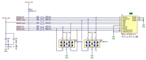
MicroSD Card Circuit
| Signal Name | Connection Method | Description |
|---|---|---|
| SDMMC0_D[3:0] | 22Ω resistor in series / use the internal pull-up resistor of the corresponding IO | SD data transmission and reception |
| SDMMC0_CLK | 22Ω resistor in series / pull-down | SD clock transmission |
| SDMMC0_CMD | 22Ω resistor in series / use the internal pull-up resistor of the corresponding IO | SD command transmission and reception |
| SDMMC0_DET | 100Ω resistor in series / use the internal pull-up resistor of the corresponding IO | SD card insertion detection |
💡 Schematic Design Notes
SDMMC_CLKalready has a 22Ω resistor connected in series on the core board (SoM), so it does not need to be added again on the baseboard (carrier board).- The
SDMMC_D[3:0],SDMMC_CMD,SDMMC_CLK, andSDMMC_DETsignals must have ESD protection devices placed near the TF card interface. If SD3.0 mode is supported, the junction capacitance of the ESD device must be less than 1pF. If only SD2.0 mode is supported, the junction capacitance requirement can be relaxed to 9pF.- Because the SDMMC and JTAG functions are multiplexed (shared pins), adjustment through the
SDMMC_DET_Lpin is required when using the SDMMC function. This switching is determined during boot, and after the system has booted, it is handled by system control. This pin is internally pulled up by default and is pulled down to Low level when a TF card is inserted.
1.1 PCB Design Recommendations
All protection devices should be placed as close as possible to the TF card interface.
SDIO routing requirements:
| Parameter | SDIO Requirement |
|---|---|
| Trace impedance | Single-ended 50Ω ±10% |
| Length matching between clock and data | < 120mil |
| Trace length | < 4 inches |
| Clearance between SDIO signal traces | At least 2 times the SDIO trace width |
2. USB3.0 Host Circuit
The RV1126B provides a total of two sets of USB 2.0 signals and one set of USB 3.0 signals. The current development board uses a solution in which USB 2.0 DRD is used as the firmware flashing interface, while USB 2.0 HOST and USB 3.0 DRD are combined to form one USB 3.0 HOST interface.
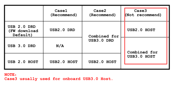
USB Multiplexer
2.1 Schematic Design Recommendations
In this development design, a USB3.0 hub chip (HUB IC) is used to expand the USB3.0 ports.
Refer to the following schematic (or wiring diagram).
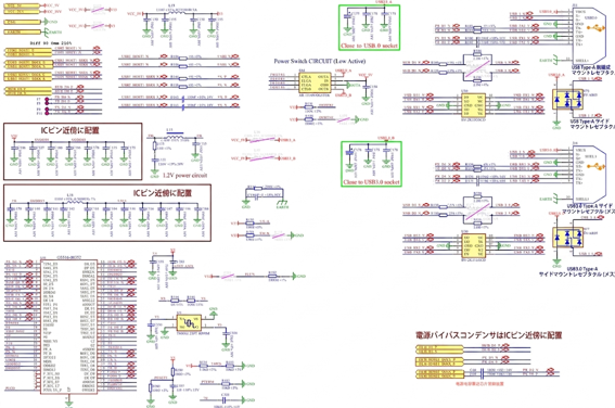
USB3.0 Hub Circuit
| Signal | Default Pull-up/Pull-down | Connection Method | Description |
|---|---|---|---|
| USB_HOST_DM / USB_HOST_DP | None | 0Ω resistor in series | Data input/output in USB HS/FS/LS modes |
| USB3_HOST_SSRX1N / USB3_HOST_SSRX1P | None | 0Ω resistor in series | Data input in USB SS mode |
| USB3_HOST_SSTX1N / USB3_HOST_SSTX1P | None | 100nF capacitor in series | Data output in USB SS mode |
💡 Schematic Design Suggestions
- To improve anti-static and surge capability, make sure to reserve footprints for ESD protection devices on the signal lines. The ESD parasitic capacitance of USB 2.0 signals must not exceed 3pF.
- To suppress electromagnetic radiation (EMI), consider placing common-mode choke coils on the signal lines. During debugging, install either resistors or common-mode choke coils according to the actual situation.
- It is recommended to add a current-limit switch to the 5V power supply. The current-limit value can be adjusted according to application requirements.
2.2 PCB Design Recommendations
All ESD protection devices should be placed as close as possible to the USB interface. The routing requirements for USB 2.0 and USB 3.0 are as follows.
Table: USB 2.0 Routing Requirements
| Parameter | USB 2.0 Routing Requirement |
|---|---|
| Trace impedance | Differential 90Ω ±10% |
| Maximum delay difference (skew) within a differential pair | < 20mil |
| Trace length | < 6 inches |
| Number of vias allowed for each signal | Recommended within 4 vias (maximum 6 vias) |
Table: USB 3.0 Routing Requirements
| Parameter | USB 3.0 Routing Requirement |
|---|---|
| Trace impedance | Differential 90Ω ±10% |
| Maximum delay difference (skew) within a differential pair | < 6mil |
| Trace length | < 6 inches |
| Capacitor requirement | 100nF ±20% (0201 package recommended) |
| Clearance between differential pairs | Recommended to be at least 4 times the USB trace width |
| Clearance between USB and other signal traces | Recommended to be at least 4 times the USB trace width |
| Number of vias allowed for each signal | Recommended within 2 vias |
| ESD device I/O-to-ground capacitance | 0.2pF or less |