
4. Multimedia
1 MIPI DSI Circuit
The RV1126B includes a MIPI DPHY DSI TX, supports MIPI version V1.2, provides a total of 4 lanes, and supports a maximum transmission rate of 1.5Gbps/Lane. The maximum resolution is 1920x1080@60Hz.
💡Notes for MIPI DPHY DSI TX interface design:
- Supports 1/2/4 Lane modes. In 1-lane mode, the default lane is D0; in 2-lane mode, the default lanes are D0/D1.
- MIPI data lanes do not support lane-to-lane swapping and must be connected one-to-one. P/N polarity swapping within a lane is also not supported.
- When connecting boards through a connector (BtoB), it is recommended to insert series resistors (2.2Ω as a reference value; the final value should meet SI test requirements) and reserve footprints for TVS diodes.
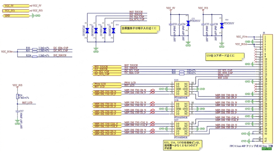
MIPI DSI Circuit
Table: MIPI DSI Signal Description
| Signal | Connection Method | Description |
|---|---|---|
| MIPI_DPHY0_TX_D0N / MIPI_DPHY0_TX_D0P | Direct connection. To suppress electromagnetic radiation (EMI), it is recommended to reserve footprints for common-mode chokes. | MIPI_DPHY0_TX data Lane0 output |
| MIPI_DPHY0_TX_D1N / MIPI_DPHY0_TX_D1P | Direct connection. To suppress electromagnetic radiation (EMI), it is recommended to reserve footprints for common-mode chokes. | MIPI_DPHY0_TX data Lane1 output |
| MIPI_DPHY0_TX_D2N / MIPI_DPHY0_TX_D2P | Direct connection. To suppress electromagnetic radiation (EMI), it is recommended to reserve footprints for common-mode chokes. | MIPI_DPHY0_TX data Lane2 output |
| MIPI_DPHY0_TX_D3N / MIPI_DPHY0_TX_D3P | Direct connection. To suppress electromagnetic radiation (EMI), it is recommended to reserve footprints for common-mode chokes. | MIPI_DPHY0_TX data Lane3 output |
| MIPI_DPHY0_TX_CLKN / MIPI_DPHY0_TX_CLKP | Direct connection. To suppress electromagnetic radiation (EMI), it is recommended to reserve footprints for common-mode chokes. | MIPI_DPHY0_TX clock output |
| MIPI_DSI0_PWM | Direct connection | Display backlight brightness control signal |
| MIPI_DSI0_RST | Pull-up | Display reset signal |
| RST_TOUCH | Pull-up | Capacitive touch panel reset signal |
| INT_TOUCH | Pull-up | Capacitive touch panel interrupt signal |
| I2C_SCL_TP0 | Pull-up | Capacitive touch panel I2C clock signal |
| I2C_SDA_TP0 | Pull-up | Capacitive touch panel I2C data signal |
1.1 PCB Design Recommendations
- All ESD protection devices should be placed at the interface location.
- The I2C clock signal should be separately protected with a ground guard (GND shield/ground copper guard). To prevent external radiation interference, add at least one GND via every 200mil.
Table: Routing Requirements - MIPI-DPHY
| Parameter | Requirement |
|---|---|
| Routing impedance | Differential 100Ω ±10% (select the target impedance of 100Ω first; if the PCB stack-up cannot meet 100Ω, ensure at least 95Ω ±10% impedance.) |
| Maximum delay difference within a differential pair (skew) | < 6mil |
| Length matching between clock and data | < 12mil |
| Routing length | < 6 inches |
| Allowed number of vias per signal | 4 or fewer recommended |
| Clearance between differential pairs (Air gap) | Recommended to be at least 4 times the MIPI trace width, and at minimum 3 times the MIPI trace width |
| Clearance between MIPI and other signal traces (Air gap) | Recommended to be at least 4 times the MIPI trace width, and at minimum 3 times the MIPI trace width |
2 MIPI CSI Circuit
The RV1126B provides two MIPI CSI RX inputs. Both support MIPI version V1.2, with a maximum transmission rate of 2.5Gbps/Lane per lane. In actual applications, the 1x4 lanes of each port can be split into 2x2-lane inputs, allowing up to four MIPI CSI RX inputs to be supported simultaneously. However, because only two MIPI CSI CLK signals are routed out from the core board (SoM), only two MIPI CSI RX inputs are supported in practice.
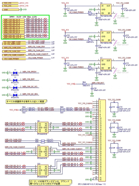
MIPI CSI Circuit
Table: MIPI CSI Signals
| Signal | Connection Method | Overview |
|---|---|---|
| MIPI_CSI0_RX_D0P MIPI_CSI0_RX_D0N | Direct connection. To suppress radiated noise (EMI), it is recommended to reserve footprints for common-mode chokes. | MIPI CSI0 data lane0 input |
| MIPI_CSI0_RX_D1P MIPI_CSI0_RX_D1N | Direct connection. To suppress radiated noise (EMI), it is recommended to reserve footprints for common-mode chokes. | MIPI CSI0 data lane1 input |
| MIPI_CSI0_RX_D2P MIPI_CSI0_RX_D2N | Direct connection. To suppress radiated noise (EMI), it is recommended to reserve footprints for common-mode chokes. | MIPI CSI0 data lane2 input |
| MIPI_CSI0_RX_D3P MIPI_CSI0_RX_D3N | Direct connection. To suppress radiated noise (EMI), it is recommended to reserve footprints for common-mode chokes. | MIPI CSI0 data lane3 input |
| MIPI_CSI0_RX_CLK0P MIPI_CSI0_RX_CLK0N | Direct connection. To suppress radiated noise (EMI), it is recommended to reserve footprints for common-mode chokes. | MIPI CSI0 clock0 input |
| MIPI_CSI0_CLK | Direct connection | MIPI CSI0 master clock |
| MIPI_CSI0_PWDN | Direct connection | MIPI CSI0 enable signal |
| MIPI_CSI0_RST | Pull-up | MIPI CSI0 reset signal |
2.1 PCB Design Notes (Common MIPI)
- The I2C clock signal must be separately shielded with ground (GND guard trace/ground copper guard). To prevent external radiation interference, add at least one GND via every 200mil.
- The MIPI_CSI routing requirements are as follows:
| Parameter | Requirement |
|---|---|
| Routing impedance | Differential 100Ω ±10% (The target impedance should preferably be 100Ω. Even if 100Ω is difficult to achieve due to the PCB layer stack-up, at least 95Ω ±10% must be met.) |
| Maximum delay difference within a differential pair (intra-pair skew) | < 6mil |
| Length matching between clock and data (inter-pair skew) | < 12mil |
| Routing length | < 6inch |
| Allowed number of vias per signal | 4 or fewer recommended |
| Gap between differential pairs (Airgap) | Recommended to be at least 4 times the MIPI trace width. At minimum, ensure 3 times. |
| Gap between MIPI and other signals (Airgap) | Recommended to be at least 4 times the MIPI trace width. At minimum, ensure 3 times. |
3. Audio Circuit
3.1 DSM Audio Interface Circuit
DSM (Digital Signal Modulator) audio directly converts audio PCM data into a 1-bit signal stream for output. The digital signal output from the interface is processed through an RC low-pass filter and then output as an analog audio signal.
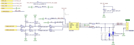
DSM Audio Interface Circuit
DSM Audio Interface Signals
| Signal | Connection Method | Description |
|---|---|---|
| DSM_AUD_RP | Connect an RC low-pass filter in series | DSM output right-channel P terminal |
| DSM_AUD_RN | Connect an RC low-pass filter in series | DSM output right-channel N terminal |
DSM audio interface design notes:
- Do not remove the RC filter circuit at the DSM output.
- The differential audio output cannot be split into two single-ended audio outputs for use. Also, because sound quality will degrade, single-ended mode is not recommended.
- SAI2_SDO is internally connected to the DSM module. Therefore, when using the DSM module, the external SAI2_SDO cannot be used.
3.1.1 PCB Design Recommendations
- Audio signals should be isolated from high-speed digital signals.
- An independent audio ground (solid ground plane) should be provided for the entire audio section.
3.2 MIC (Microphone) Circuit
The main board integrates one set of MIC differential input interfaces. It supports both differential and single-ended MIC inputs. The figure below shows the reference circuit for differential MIC input.
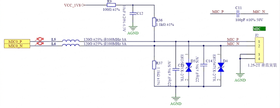
Microphone Circuit
Table: Earphone Circuit Signal Description
| Signal | Connection Method | Description |
|---|---|---|
| MIC0_P | Connect a resistor and capacitor (RC) in series | AUDIO ADC differential signal MICP input |
| MIC0_N | Connect a resistor and capacitor (RC) in series | AUDIO ADC differential signal MICN input |
Audio ADC interface design notes:
- The MIC differential input cannot be split into two single-ended inputs for use.
- All input interfaces can be used as LINE_IN or MIC_IN input channels. If the input device is a passive MIC (such as a condenser microphone), a 1.8V bias voltage must be supplied. This is not required for active input devices.
- Reserve an RC circuit for the MIC input bias voltage to improve power supply noise.
3.2.1 PCB Design Recommendations
- Audio signals should be isolated from high-speed digital signals.
- An independent audio ground (solid ground plane) should be provided for the entire audio section.