
5. Connectivity and Network
1. Gigabit Ethernet Circuit
The RV1126B chip integrates one GMAC controller. It can provide an RMII/RGMII interface to expand an external Ethernet PHY chip, or switch to the built-in FEPHY. These two options cannot be used at the same time [cite: 1]. It supports a 10/100/1000 Mbps RGMII interface [cite: 1].
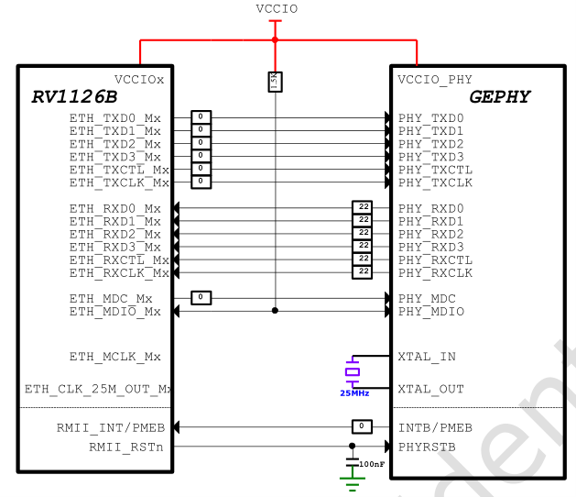
Gigabit Ethernet Circuit
RGMII Signal Description
| Signal | Connection Method | Description |
|---|---|---|
| RGMII_TXD0 / RGMII_TXD1 / RGMII_TXD2 / RGMII_TXD3 | Reserved 0Ω resistor in series, placed near the RV1126B side | Data transmission |
| RGMII_TXEN | Reserved 0Ω resistor in series, placed near the RV1126B side | Data transmit enable on the rising edge and data transmit error on the falling edge |
| RGMII_TXCLK | Reserved 0Ω resistor in series, placed near the RV1126B side | Data transmit reference clock |
| RGMII_RXD0 / RGMII_RXD1 / RGMII_RXD2 / RGMII_RXD3 | 22Ω resistor in series, placed near the PHY side | Data reception |
| RGMII_RXDV_CRS | 22Ω resistor in series, placed near the PHY side | Data receive valid on the rising edge and receive error on the falling edge |
| RGMII_RXCLK | 22Ω resistor in series, placed near the PHY side | Data receive reference clock |
| ETH0_REFCLKO_25M | Reserved 0Ω resistor in series, placed near the RK3588 side | RK3588 provides a 25MHz clock instead of using the PHY crystal oscillator |
| RGMII_MCLKINOUT | Output mode: reserved 0Ω resistor in series, placed near the RK3588 side Input mode: 22Ω resistor in series, placed near the PHY side | PHY sends 125MHz to MAC, optional |
| RGMII_MDC | Reserved 0Ω resistor in series, placed near the RK3588 side | Management data clock |
| RGMII_MDIO | External 1.5k–1.8kΩ pull-up resistor | Management data input/output |
| RGMII_RSTn_L | Pull-up | PHY reset signal |
Notes for RGMII/RMII Interface Design:
- In GMII mode, delay lines are integrated into the TX/RX clock paths inside the RV1126B chip and support adjustment [cite: 1]. In the default settings of the reference schematic, the timing between TXCLK and data is controlled by the MAC, and the timing between RXCLK and data is controlled by the PHY. For example, when using 8211F/FI, RXCLK has a 2ns delay enabled by default. Pay attention to this setting when using other PHYs [cite: 1].
- The reset signal of the Ethernet PHY must be controlled by a GPIO, and the GPIO voltage level must match the PHY I/O voltage level [cite: 1]. To improve ESD immunity, add a 100nF capacitor near the PHY pin [cite: 1]. Note: the reset pin of 8211F/FI only supports 3.3V level [cite: 1].
- INTB/PMEB of 8211F/FI is an open-drain output, so an external pull-up resistor must be added [cite: 1].
- If the PHY uses an external crystal oscillator, select the crystal capacitors according to the load capacitance of the actual crystal oscillator, and keep the frequency deviation within +/-20ppm [cite: 1].
- The external resistor connected to the RSET pin of 8211F/FI must be 2.49kΩ with 1% accuracy and must not be changed arbitrarily [cite: 1].
- The PHY hardware initialization settings must match the actual requirements [cite: 1].
- MDIO requires an external pull-up resistor. A value of 1.5k–1.8kΩ is recommended [cite: 1]. The pull-up power supply must also match the I/O power supply [cite: 1].
- The connection of the center tap of the transformer, or Ethernet transformer, must follow the reference design of each Ethernet PHY vendor [cite: 1]. Different PHY vendors may use different connection methods [cite: 1].
- The 1000pF isolation capacitor should be a high-voltage safety-rated capacitor. It is recommended to provide sufficient creepage distance, or electrical clearance, to ensure lightning protection safety [cite: 1].
- For the 75Ω resistor on the high-voltage side of the Ethernet transformer, an 0805 package or larger is recommended [cite: 1].
- To achieve a lightning protection level above 4KV, a surge arrester must be added [cite: 1]. A standard isolation transformer can usually only meet the 2KV level requirement [cite: 1].
- If differential-mode lightning testing is required, add TVS diodes between the MDI differential pairs [cite: 1].
- Be sure to confirm that the RJ45 package, or footprint, matches the schematic [cite: 1]. RJ45 connectors have both “Tab down” and “Tab up” types, and their signal order is exactly reversed [cite: 1]. When using 8211F/FI, the “Tab down” type is recommended so that the MDI routing order is aligned [cite: 1].
PCB Design Description:
- The reset signal is susceptible to interference and must be separated from high-speed signals [cite: 1].
- Prioritize the placement of the crystal oscillator circuit. To avoid vias, place it on the same layer as the chip and as close as possible to the chip [cite: 1]. The crystal routing must be fully surrounded by ground [cite: 1].
| Parameter | Requirement |
|---|---|
| Routing impedance | Single-ended 50Ω ±10% |
| Length matching between (TXD-3, TXEN) and TXCLK | < 120mil |
| Length matching between (RXD-3, RXDV) and RXCLK | < 120mil |
| Routing length | < 5 inches |
| Spacing, or air gap, between RGMII signal traces | Recommended to be at least 2 times the RGMII trace width |
| Spacing, or air gap, between RGMII and other signal traces | Recommended to be 3 times the RGMII trace width, and at least 2 times the RGMII trace width |
7. WiFi + Bluetooth Circuit
The mainboard WiFi module uses the Lierda DB37 module, which supports WiFi 6 + Bluetooth + StarFlash [cite: 1]. It supports IEEE 802.11b/g/n/ax@2.4G, BLE5.2, and SLE1.0 standard communication protocols, and provides an SDIO 2.0 interface [cite: 1].
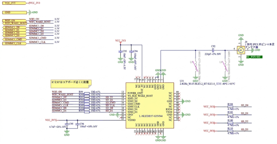
WiFi + Bluetooth Circuit
WiFi + Bluetooth Signal Description
| Signal | Connection Method | Description |
|---|---|---|
| SDMMC0_D[3:0] | 33Ω resistor in series, with a 4.7kΩ pull-up resistor | SD data transmission and reception |
| SDMMC0_CLK | 33Ω resistor in series | SD clock transmission |
| SDMMC0_CMD | 33Ω resistor in series, using the internal pull-up resistor of the corresponding I/O | SD command transmission and reception |
| WIFI_WAKE_HOST_H | Direct connection | CPU wake-up from Wi-Fi |
| WIFI_ON | Direct connection | Wi-Fi module power enable |
PCB Design Description:
SDIO Routing Description
| Parameter | Requirement |
|---|---|
| SDIO routing impedance | Single-ended 50Ω ±10% |
| Length matching between clock and data | < 120mil |
| Routing length | < 4 inches |
| Spacing between SDIO signal traces | At least 2 times the SDIO trace width |
8. MINI-PCIE Interface Circuit
The mainboard supports one MINI-PCIE interface. It supports USB 2.0 signals and SIM card slot signals, but does not support PCIE signals [cite: 1]. USB-signal 4G modules and similar devices can be inserted [cite: 1]. The power supply uses an independent DC-DC power module and supports up to 2A [cite: 1].
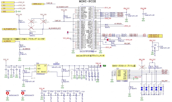
MINI-PCIE Interface Circuit
MINI-PCIE Interface Description
| Signal | Connection Method | Description |
|---|---|---|
| WAKEUP_OUT | Pull-up | Sleep control. Low level indicates sleep state, and high level indicates wake-up |
| r | 2.2Ω resistor in series | Data input/output in USB HS/FS/LS modes |
| PCIE_HOST4_DP | 2.2Ω resistor in series | Same as above |
| 4G_RESET | Pull-up | Module reset signal |
PCB Design Description:
USB 2.0 Routing Description
| Parameter | Requirement |
|---|---|
| USB 2.0 routing impedance | Differential 90Ω ±10% |
| Maximum routing length difference, or skew, within a differential pair | < 20mil |
| Routing length | < 6 inches |
| Number of vias allowed for each signal | Recommended to be 4 or fewer, and must not exceed 6 |