
RV1126B Evaluation Board Hardware Specification
1. Function Overview
1.1 Product Overview
RV1126B-Nano-TB is an AIoT motherboard for the AIoT field. The core board is based on the Rockchip RV1126B processor design. It integrates four Cortex-A53 cores and an independent NEON coprocessor, supports 4K@30fps H.264/H.265 decoding, and also supports 4K@30fps H.264/H.265 encoding. It introduces a new-generation, fully hardware-based ISP (image signal processor) with up to 12 megapixels, providing various algorithm accelerators such as HDR, 3A, LSC, 3DNR, 2DNR, sharpening, dehazing, fisheye correction, gamma correction, and feature point detection. At the same time, as a supplement to the traditional ISP, it also introduces an AI-ISP with up to 8 megapixels, providing excellent spatial noise reduction performance and powerful image enhancement. The built-in NPU delivers up to 3 TOPS of computing power and supports mixed INT4/INT8/INT16/FP16 operations. A complete Linux development package is provided for customer secondary development.
1.2 Product Images
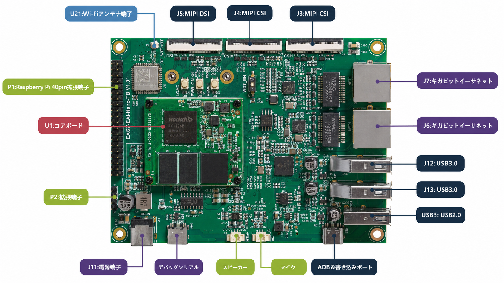
Figure 1 Front View of the Product
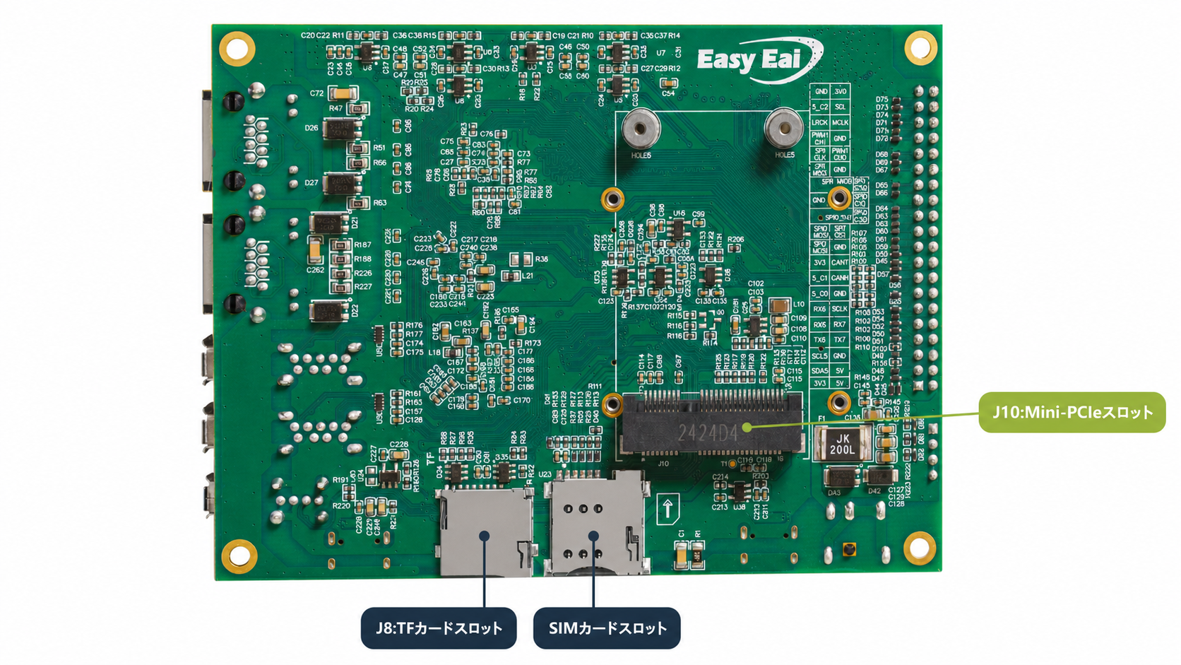
Figure 2 Rear View of the Product
1.3 Product Features
Table 1 Product Features
| Name | RV1126B Nano-TB | RV1126B Nano-TBI |
|---|---|---|
| Processor | RV1126B | RV1126BJ |
| Core | 4×ARM Cortex-A53@1.6GHz | 4×ARM Cortex-A53@1.6GHz |
| NPU | Supports INT4/INT8/INT16/FP16 mixed operations, computing power up to 3 TOPS | Supports INT4/INT8/INT16/FP16 mixed operations, computing power up to 3 TOPS |
| VPU | 4K@30fps H.264/H.265 Decoder 4K@30fps H.264/H.265 Encoder | 4K@30fps H.264/H.265 Decoder 4K@30fps H.264/H.265 Encoder |
| ISP | 12M ISP+8M AI-ISP | 12M ISP+8M AI-ISP |
| OS | Debian12/Ubuntu22.04 | Debian12/Ubuntu22.04 |
| Memory | 1/2GB DDR4 | 1/2GB DDR4 |
| eMMC Storage | 64GB EMMC | 8/16GB EMMC |
| MIPI DSI | 1-channel 4-Lane MIPI DSI, 1.5Gbps/lane | 1-channel 4-Lane MIPI DSI, 1.5Gbps/lane |
| MIPI CSI | 2 channels, each supporting 4 lanes, 2.5Gbps/Lane | 2 channels, each supporting 4 lanes, 2.5Gbps/Lane |
| TF Card | 1-channel TF card interface | 1-channel TF card interface |
| USB 3.0 Host | 2-channel USB3.0 TYPE-A interface | 2-channel USB3.0 TYPE-A interface |
| USB 2.0 Host | 1-channel USB2.0 TYPE-A interface | 1-channel USB2.0 TYPE-A interface |
| Type-C | 1-channel firmware download interface | 1-channel firmware download interface |
| Ethernet | 2-channel Gigabit Ethernet | 2-channel Gigabit Ethernet |
| WiFi | 1-channel WiFi6 | 1-channel WiFi6 |
| Bluetooth | 1-channel Bluetooth 5.2 | 1-channel Bluetooth 5.2 |
| NearLink (SparkLink) | 1-channel NearLink communication SLE1.0 | 1-channel NearLink communication SLE1.0 |
| Microphone | 1-channel microphone input | 1-channel microphone input |
| Speaker | 1-channel 3W/4Ω speaker | 1-channel 3W/4Ω speaker |
| UART | 2 channels, 3.3V | 2 channels, 3.3V |
| CAN | 1 channel, 3.3V | 1 channel, 3.3V |
| I2C | 1 channel | 1 channel |
| PWM | 2 channels | 2 channels |
| SPI | 2 channels | 2 channels |
| SAI | 1 channel | 1 channel |
| GPIO | 3 channels | 3 channels |
| Debug Serial Port | 1 channel | 1 channel |
| Indicator LED | 1 power indicator | 1 power indicator |
| Button | 1 reset button, 1 LOAD button, 1 PWRON power button | 1 reset button, 1 LOAD button, 1 PWRON power button |
| Watchdog | Supports external hardware watchdog | Supports external hardware watchdog |
| Supply Voltage | DC 12V voltage input | DC 12V voltage input |
| Mechanical Dimensions | 120mm (length) *90mm (width) | 120mm (length) *90mm (width) |
| Environmental Test | -20℃ ~ +85℃ | -40℃ ~ +85℃ |
2. Resource Introduction
2.1 Processor RV1126B
The Rockchip RV1126B processor integrates four Cortex-A53 cores and an independent NEON coprocessor. It supports 4K@30fps H.264/H.265 decoding and also supports 4K@30fps H.264/H.265 encoding. It includes built-in RGA 2D graphics acceleration. The built-in NPU supports INT4/INT8/INT16/FP16 mixed operations, with computing power up to 3 TOPS. Network models based on frameworks such as TensorFlow, MXNet, PyTorch, and Caffe can be easily converted.
2.2 Display Interface
The RV1126B motherboard integrates one MIPI DSI 4-Lane output interface.
2.2.1 MIPI DSI
The motherboard integrates one MIPI DSI interface, supports D-PHY V2.0, and provides a maximum transmission speed of 1.5Gbps/Lane. It supports up to 1920x1080@60Hz and RGB (up to 24 bits) format. The physical interface is a 40-pin, 0.5mm-pitch horizontal FPC connector, as shown in Table 3. The reference designator of MIPI DSI is J5.
Table 3 MIPI DSI Display Interface Pin Overview
| Pin No. | Signal Name | Function | Pin No. | Signal Name | Function |
|---|---|---|---|---|---|
| 1 | VCC5V | 5V power supply | 2 | VCC5V | 5V power supply |
| 3 | GND | System ground | 4 | VDD_3V3 | 3.3V power supply |
| 5 | VDD_3V3 | 3.3V power supply | 6 | NC | NC |
| 7 | NC | NC | 8 | NC | NC |
| 9 | NC | NC | 10 | NC | NC |
| 11 | NC | NC | 12 | GND | System ground |
| 13 | RST_TOUCH | Touchscreen reset signal | 14 | INT_TOUCH | Touchscreen interrupt signal |
| 15 | I2C_SCL | I2C clock signal | 16 | I2C_SDA | I2C data signal |
| 17 | PWM_LCD | Backlight brightness control signal | 18 | RST_LCD | Display reset signal |
| 19 | GND | System ground | 20 | NC | NC |
| 21 | NC | NC | 22 | NC | NC |
| 23 | NC | NC | 24 | GND | System ground |
| 25 | MIPI_DSI_D0N | Display signal channel 0 negative | 26 | MIPI_DSI_D0P | Display signal channel 0 positive |
| 27 | GND | System ground | 28 | MIPI_DSI_D1N | Display signal channel 1 negative |
| 29 | MIPI_DSI_D1P | Display signal channel 1 positive | 30 | GND | System ground |
| 31 | MIPI_DSI_D2N | Display signal channel 2 negative | 32 | MIPI_DSI_D2P | Display signal channel 2 positive |
| 33 | GND | System ground | 34 | MIPI_DSI_CLKN | Display clock signal negative |
| 35 | MIPI_DSI_CLKP | Display clock signal positive | 36 | GND | System ground |
| 37 | MIPI_DSI_D3N | Display signal channel 3 negative | 38 | MIPI_DSI_D3P | Display signal channel 3 positive |
| 39 | GND | System ground | 40 | GND | System ground |
2.3 Image Input Interface
The motherboard image input interface includes two MIPI CSI channels, enabling two HD video signal inputs. The processor includes powerful 4K@30fps H.264 and H.265 encoders, enabling HD video encoding processing.
2.3.1 MIPI CSI
The motherboard integrates two MIPI CSI interfaces and supports D-PHY V1.2. Each interface has 4 lanes, with a maximum transmission speed of 2.5Gbps/Lane. The physical interface is a 40-pin, 0.5mm-pitch horizontal FPC connector. The signal definitions of the two interfaces are the same, as shown in Table 4. The two MIPI CSI interfaces are identified on the motherboard by the silkscreens “MIPI CSI0” (reference designator J3) and “MIPI CSI1” (reference designator J4).
Table 4 MIPI CSI Interface Description
| Pin No. | Signal Name | Function | Pin No. | Signal Name | Function |
|---|---|---|---|---|---|
| 1 | NC | Not connected | 2 | VCC_2V8 | Not connected |
| 3 | NC | Not connected | 4 | NC | Not connected |
| 5 | I2C_SCL | I2C clock pin | 6 | I2C_SDA | I2C data pin |
| 7 | GND | Digital ground | 8 | NC | Not connected |
| 9 | GND | Digital ground | 10 | NC | Not connected |
| 11 | NC | Not connected | 12 | GND | Digital ground |
| 13 | MIPI_CSI_RX_D2P | Data differential 2+ | 14 | MIPI_CSI_RX_D2N | Data differential 2- |
| 15 | GND | Digital ground | 16 | MIPI_CSI_RX_D3P | Data differential 3+ |
| 17 | MIPI_CSI_RX_D3N | Data differential 3- | 18 | GND | Digital ground |
| 19 | VCC_1V8 | 1.8V power output | 20 | NC | Not connected |
| 21 | NC | Not connected | 22 | NC | Not connected |
| 23 | VCC_1V2 | 1.2V power output | 24 | MIPI_CSI_PWDN | Enable pin |
| 25 | MIPI_CSI_RST | Reset pin | 26 | GND | Digital ground |
| 27 | MIPI_CSI_CLK | Main clock | 28 | GND | Digital ground |
| 29 | MIPI_CSI_RX_CLKP | Clock differential + | 30 | MIPI_CSI_RX_CLKN | Clock differential - |
| 31 | GND | Digital ground | 32 | MIPI_CSI_RX_D0P | Data differential 0+ |
| 33 | MIPI_CSI_RX_D0N | Data differential 0- | 34 | GND | Digital ground |
| 35 | MIPI_CSI_RX_D1P | Data differential 1+ | 36 | MIPI_CSI_RX_D1N | Data differential 1- |
| 37 | GND | Digital ground | 38 | NC | Not connected |
| 39 | NC | Not connected | 40 | NC | Not connected |
2.4 TF Card Slot
The motherboard integrates one TF card interface, allowing a TF card to be inserted for data storage. The reference designator is J8. It supports SDIO3.0, and the signal interface voltage is dynamically adjustable, supporting 1.8V and 3.3V. The TF card can be used as the system boot disk, and booting from the TF card is supported.
2.5 USB
The motherboard has two USB3.0 interfaces, one USB2.0 interface, and one TYPE-C interface (firmware download interface).
2.5.1 USB3.0 Interface
The motherboard has two USB3.0 TYPE-A interfaces, expanded from one USB3.0 HUB chip. The interface also includes USB 2.0 signals and is a full-function USB 3.0 interface. The physical interface is a vertical TYPE-A port, with reference designators J12 and J13.
2.5.2 USB2.0 Interface
The motherboard has one USB2.0 TYPE-A interface and supports HS/FS/LS modes. Because this interface shares one set of USB signals with the TYPE-C interface, only one of this interface and the TYPE-C interface can be selected for use at a time. The physical interface of this USB2.0 port is a TYPE-A port, with reference designator USB3.
2.5.3 TYPE-C Interface
The motherboard has one USB2.0 TYPE-C interface, which functions as the system firmware download interface. The reference designator is USB1.
2.6 Ethernet
The motherboard integrates two Gigabit Ethernet interfaces and supports automatic recognition of 10/100/1000 Mbps data transfer rates. The physical interface is an RJ45 port. The reference designator for LAN0 is J7, and the reference designator for LAN1 is J6.
2.7 WiFi, Bluetooth, and NearLink
The motherboard integrates a DB37 tri-mode wireless communication module. It supports the IEEE 802.11b/g/n/ax@2.4G, BLE5.2, and SLE1.0 standard communication protocols and supports the SDIO 2.0 interface. This module supports 802.11n 20MHz/40MHz bandwidth and 802.11ax 20MHz bandwidth, providing a physical-layer speed of up to 150Mbps and longer coverage distance. The module has one antenna interface, with an IPX socket as the physical terminal. The reference designator is U21. The WiFi and Bluetooth features are shown in Table 6.
Table 6 WiFi and Bluetooth Characteristics Description
| Name | Characteristics | Description |
|---|---|---|
| 2.4GHz WiFi | WiFi Standard | IEEE 802.11b/g/n & Wi-Fi compliant |
| Frequency Range | 2.400 GHz ~ 2.4835 GHz (2.4GHz ISM Band) | |
| Number of Channels | 2.4GHz: Ch1 ~ Ch13 | |
| Modulation Mode | 802.11b : DQPSK, DBPSK, CCK 802.11 g/n : OFDM /64-QAM, 16-QAM, QPSK, BPSK 802.11ax : OFDM /256-QAM, 64-QAM, 16-QAM, QPSK, BPSK | |
| Bluetooth | Bluetooth Standard | BLE5.2 |
| Frequency Range | 2400 MHz ~ 2483.5 MHz(2.4GHz ISM Band) | |
| Number of Channels | LE: Ch0~Ch39 | |
| Modulation Mode | GFSK | |
| NearLink (SparkLink) | NearLink Standard | SLE1.0 |
| Operating Frequency | 2400 MHz ~ 2483.5 MHz(2.4GHz ISM Band) | |
| Modulation Mode | GFSK, BPSK, QPSK |
2.8 Audio
The motherboard supports one microphone audio input and one speaker audio output.
2.9 MiniPCIE Expansion Interface
The motherboard supports one miniPCIE expansion interface, with reference designator J10. This interface supports USB2.0 signals but does not support PCIE functionality. It can be used to expand 4G communication modules with USB2.0 interfaces and other communication modules with USB interfaces.
2.10 Single-Row Pin Header Terminal
The motherboard reserves a single-row pin header, and the terminal includes ADC and UART. The interface description is shown in Table 7. The terminal pitch is 2.54mm. The reference designator is P2.
Table 7 Terminal Pin Description
| Silkscreen Description | Function Name | Function Description |
|---|---|---|
| 1 | ADC0_IN2 | ADC0 acquisition channel 2 |
| 2 | UART2_RX_M0 | Serial port 2 receive signal (3.3V) |
| 3 | UART2_TX_M0 | Serial port 2 transmit signal (3.3V) |
| 4 | GND | GND |
2.11 Expansion Pin Header Interface
The motherboard integrates an expansion pin header interface, providing resources such as ADC, I2C, and serial ports. The interface description is shown in Table 8. The terminal pitch is 2.54mm. The reference designator is P1.
Table 8 Terminal Pin Description
| Silkscreen Description | Function Name | Function Description |
|---|---|---|
| 1 | VCC_3V3 | 3.3V voltage output |
| 2 | VCC_5V | 5V voltage output |
| 3 | I2C5_SDA_M0 | I2C5 data pin (3.3V) |
| 4 | VCC_5V | 5V voltage output |
| 5 | I2C5_SCL_M0 | I2C5 clock pin (3.3V) |
| 6 | GND | System ground |
| 7 | UART6_TX_M0 | Serial port 6 transmit signal (3.3V) |
| 8 | UART7_TX_M0 | Serial port 7 transmit signal (3.3V) |
| 9 | GND | System ground |
| 10 | UART7_RX_M0 | Serial port 7 receive signal (3.3V) |
| 11 | UART6_RX_M0 | Serial port 6 receive signal (3.3V) |
| 12 | SAI1_SCLK_M2 | SAI1 serial clock signal (3.3V) |
| 13 | GPIO5_C0_D | GPIO5_C0_d (3.3V) |
| 14 | GND | System ground |
| 15 | GPIO5_C1_D | GPIO5_C1_d (3.3V) |
| 16 | CAN0_RXD_M1 | CAN receive (3.3V) |
| 17 | VCC_3V3 | 3.3V voltage output |
| 18 | CAN0_TXD_M1 | CAN transmit (3.3V) |
| 19 | SPI0_MOSI_M2 | SPI0 master output slave input (3.3V) |
| 20 | GND | System ground |
| 21 | SPI0_MISO_M2 | SPI0 master input slave output (3.3V) |
| 22 | SPI1_CSN1_M1 | SPI1 chip select signal 1 (3.3V) |
| 23 | SPI0_CLK_M2 | SPI0 clock signal (3.3V) |
| 24 | SPI0_CSN0_M2 | SPI0 chip select signal 0 (3.3V) |
| 25 | GND | System ground |
| 26 | SPI0_CSN1_M0 | SPI0 chip select signal 1 (3.3V) |
| 27 | SPI1_MOSI_M1 | SPI1 master output slave input (3.3V) |
| 28 | SPI1_CSN0_M1 | SPI1 chip select signal 0 (3.3V) |
| 29 | SPI1_MISO_M1 | SPI1 master input slave output (3.3V) |
| 30 | GND | System ground |
| 31 | SPI1_CLK_M1 | SPI1 clock signal (3.3V) |
| 32 | PWM1_CH0_M1 | PWM1 channel 0 output (3.3V) |
| 33 | PWM1_CH1_M1 | PWM1 channel 1 output (3.3V) |
| 34 | GND | System ground |
| 35 | SAI1_LRCK_M2 | SAI1 frame clock signal (3.3V) |
| 36 | SAI1_MCLK_M2 | SAI1 main clock (3.3V) |
| 37 | GPIO5_C2_D | GPIO5_C2_d (3.3V) |
| 38 | SAI1_SDI_M2 | SAI0 data input |
| 39 | GND | System ground |
| 40 | SAI1_SDO_M2 | SAI1 data output |
2.12 Indicator LEDs
The motherboard integrates two indicator LEDs, both in SMD LED form. Reference designator D79 is the power indicator LED, indicating whether the system is powered on normally. Reference designator D36 is the 4G module communication indicator LED, indicating whether 4G module communication is normal.
2.13 Buttons
The motherboard integrates three tact switches. The button descriptions are shown in Table 10.
Table 10 Button Description
| Reference Designator | Name | Description |
|---|---|---|
| S1 | RESET | Reset button |
| S2 | LOAD | Loader mode button. Hold down this button and press the reset button to enter Loader download mode |
| S4 | PWRON | Power on/off button |
2.14 Hardware Watchdog
The motherboard integrates one hardware watchdog, and the watchdog overflow time is 1.6 seconds. In other words, if the watchdog is not cleared (fed) within 1.6 seconds, the watchdog generates a reset signal to reset the system. Therefore, to prevent a system reset, the Lingmou system clears the watchdog every 0.8 seconds (≤ overflow time * 1/2). If the watchdog needs to be [disabled], open the enclosure and set “WDT” on DIP switch S3 (reference designator) to “ON”. If “WDT” on DIP switch S3 is set to “1”, the watchdog operates normally.
2.15 DC Socket
The power interface of the motherboard is a 5.5mm standard DC socket, with reference designator J11. The supply voltage is a standard 12V input, and a 12V 3A power adapter is recommended.
3. Electrical Parameters
3.1 Power Parameters
Table 11 Power Parameters
| Parameter | Supply Voltage | Supply Current | Total Power Consumption | Unit |
|---|---|---|---|---|
| Normal system startup | 12V | 0.195A | 2.34W | V/A/W |
| Enter freeze sleep mode | 12V | 0.069A | 0.828W | V/A/W |
| Enter mem sleep mode | 12V | 0.083A | 0.996W | V/A/W |
| CPU utilization 50% (2 cores fully loaded) | 12V | 0.225A | 2.70W | V/A/W |
| CPU utilization 100% (4 cores fully loaded) | 12V | 0.255A | 3.06W | V/A/W |
| CPU utilization 50% + NPU running at maximum compute load | 12V | 0.393A | 4.71W | V/A/W |
4. Mechanical Dimensions
Table 12 Mechanical Dimensions
| Parameter | Specification | Description |
|---|---|---|
| Board Length | 120mm | — |
| Board Width | 90mm | — |
| Positioning Hole Size | 3mm | Fixed using M3 screws |
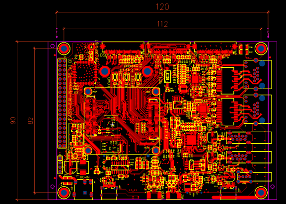
Figure 3 Mechanical Dimension Drawing