
RV1126B Minimum System
The core board integrates the power management IC, DDR, and EMMC into a compact module, so the required external circuitry is very simple. A minimum system can be built with only a 5V power supply and basic peripherals. During system power-up, always power on the core board before the baseboard to prevent reverse current from flowing into the baseboard and affecting system startup.
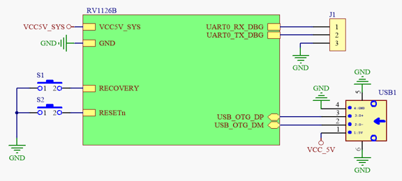
RV1126B SoM minimum system
There are four M2 positioning holes around the core board. These holes are used to fasten the core board to the baseboard standoffs with screws. The provided core board footprint includes soldering positions for the standoffs. The model is TH-1.6-3.0-M2, and the specification is M2φ4L3+1.5.
Note: For convenient debugging and upgrading, be sure to reserve the following when designing the baseboard:
-
- Recovery button and reset button
-
- Debug serial port (UART0)
-
- ADB interface (USB_OTG)
2. Reset Circuit
The reset circuit consists of a reset button and protection devices, and it directly resets the CPU and PMIC on the core board. The reset signal level is 3.3V. A 1KΩ pull-up resistor is already connected inside the core board. CPU reset requires at least 10ms.
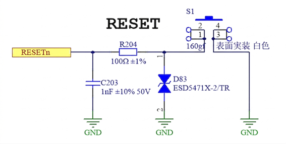
Reset signal
| Signal Name | Default Setting (Pull-up/Pull-down) | Connection Method Description (Connection Target) |
|---|---|---|
| SARADC_VIN1_KEY/RECOVERY | Pull-up to 1.8V | Directly connected to Recovery download mode (direct connection) |
| RESETn | Pull-up to 3.3V | Directly connected to the reset pins of the CPU and PMIC (direct connection) |
PCB Design Notes:
- The reset signal is susceptible to interference, so the RESETn trace should be as short as possible and kept away from strong interference sources such as DCDC and RF circuits. If the trace is long, ground shielding is recommended, and a GND via should be added every 200mil.
- CPU reset requires at least 10ms.
- Capacitor C203 should be placed near the reset pin of the core board.
- Protection device D83 should be placed near switch S1.
3. Recovery Download Mode Circuit
Button S2 is the LOAD button and is connected to the CPU’s SARADC_VIN1_KEY/RECOVERY. When the reset button is pressed while the LOAD button is held down, the system enters Loader download mode, allowing firmware to be downloaded through the flashing interface.
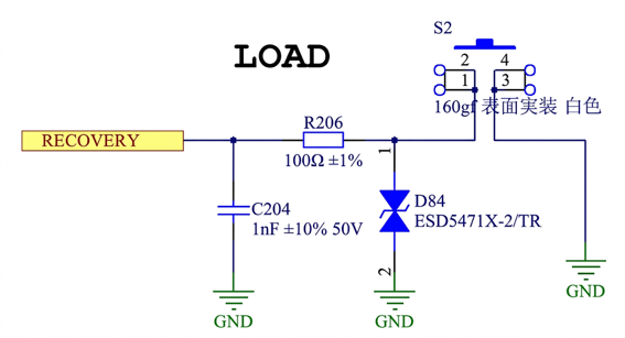
Recovery signal
| Signal Name | Default Setting (Pull-up/Pull-down) | Connection Method Description (Connection Target) |
|---|---|---|
| SARADC_VIN1_KEY/RECOVERY | Pull-up to 1.8V | Directly connected to Recovery download mode (direct connection) |
PCB Design Notes:
- The SARADC_VIN1_KEY/RECOVERY signal should be kept away from high-speed signals. Routing on adjacent layers near high-speed signals and layer changes through vias near high-speed signals are prohibited. It should also not cross any inductor area.
- Protection device D84 should be placed near button S2.
4. Maskrom Download Mode Circuit
The Maskrom interface is brought out through a test point on the core board and is connected to the CPU’s BOOT_SARADC_IN0. When the Maskrom interface is shorted and the reset button is pressed, the system enters Maskrom download mode. This mode is usually used only when the system firmware is damaged and the board is “bricked.” Use Loader mode for normal firmware downloads.
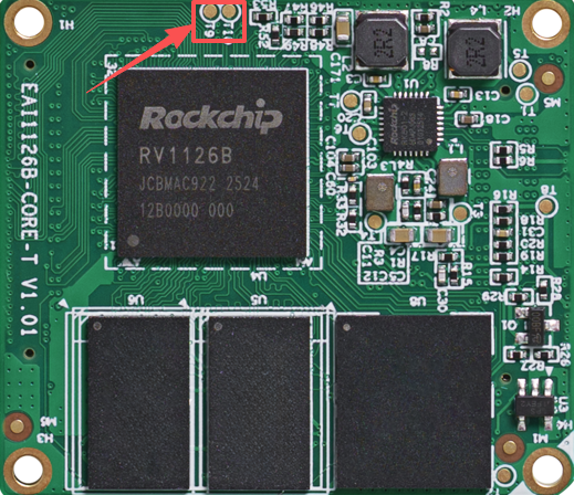
MaskROM test point location
| Signal Name | Default Setting (Pull-up/Pull-down) | Connection Method Description (Connection Target) |
|---|---|---|
| BOOT_SARADC_IN0 | Pull-up to 1.8V | Directly connected to Maskrom download mode (direct connection) |
5. Debug Serial Port
UART0 is the system debug serial port. It can output all interaction information and also accepts shell command input. It cannot be used as a general-purpose serial port. On the EASY-EAI-Nano-TB mainboard, a CH340C conversion chip is added to convert UART0 to USB signals. It can be connected to a PC simply by inserting a TYPE-C cable. The voltage level is 3.3V.
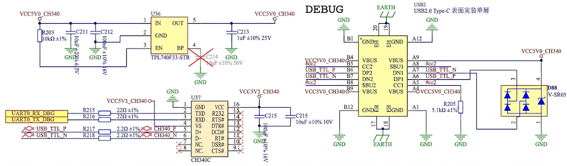
Debug UART circuit
| Signal (Signal) | Connection Method (Connection Method) | Description (Description) |
|---|---|---|
| UART0_RX_DBG | 22Ω buffer resistor (damping resistor) connected in series | Serial port receive signal |
| UART0_TX_DBG | 22Ω buffer resistor (damping resistor) connected in series | Serial port transmit signal |
5.1 PCB Design Recommendations
- Protection components (D83, ED27) should be placed near the USB connector.
- USB 2.0 routing requirements:
| Parameter | Specification Requirement (Specification) |
|---|---|
| USB 2.0 trace impedance | Differential 90Ω ±10% |
| Intra-pair length difference (skew) | < 20mil |
| Trace length | < 6 inch |
| Allowed number of vias per signal | Recommended 4 or fewer, maximum 6 |
6. TYPE-C Flashing Interface
This interface is used for firmware downloads and application debugging. USB30_OTG0_VBUSDET is the USB OTG insertion detection pin, and the detection voltage is 3.3V. The USB30_OTG0_ID pin is used to switch between Host and Device modes. High level indicates Device mode, and low level indicates Host mode. Because it is pulled up internally to 1.8V in the CPU, the default mode is Device mode.
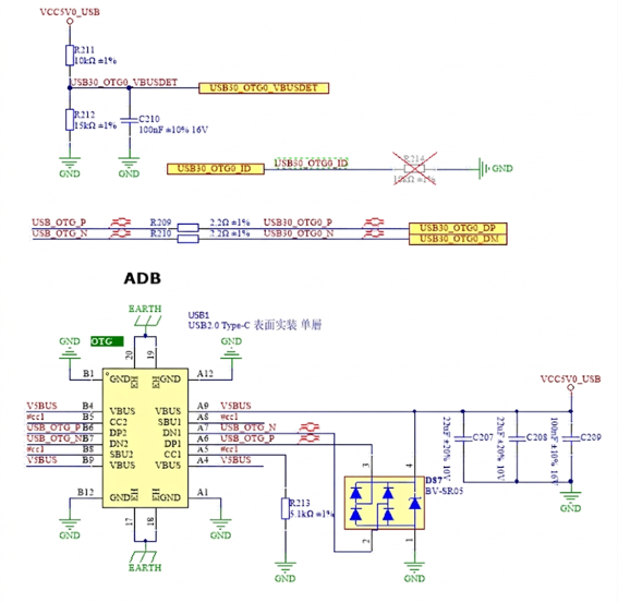
Type-C flashing interface circuit
| Signal Name (Signal Name) | Connection Method (Connection Method) | Description (Description) |
|---|---|---|
| USB_OTG_N | 2.2Ω resistor connected in series | Data input/output in USB HS/FS/LS mode |
| USB_OTG_P | 2.2Ω resistor connected in series | Data input/output in USB HS/FS/LS mode |
| USB30_OTG0_ID | Directly connected to the OTG0 ID signal | OTG0 ID signal |
| USB30_OTG0_VBUSDET | Detection through resistor divider | OTG0 insertion detection signal |